


Precision Laser Marking for Electronics and Semiconductors
I once picked up a failed microchip from a scrap board in a small repair lab in Ontario. Under a loupe, the serial number on its tiny 4 mm × 4 mm surface was flawless—perfect spacing, crisp edges, and no visible thermal damage to the surrounding material. That mark had been applied in milliseconds using a UV laser. The chip itself had likely moved through multiple countries before ending up on that workbench, yet that microscopic code made its entire journey traceable.

That moment captures why laser marking has become the standard across electronics manufacturing—from semiconductor fabrication to PCB assembly and final device production. In Canada’s growing electronics, clean-tech, and advanced manufacturing sectors, the shift away from ink printing and labels toward laser marking is driven by a simple reality: only laser marks can survive the full lifecycle of electronic components.
Why Laser Marking Has Become the Industry Standard
Electronics manufacturing presents unique challenges that traditional marking methods simply can’t handle:
- Extremely small surfaces (often millimetres or less)
- Diverse materials (polymers, metals, ceramics, silicon)
- High heat sensitivity
- Strict traceability requirements across supply chains
Traditional methods fail under these conditions:
| Traditional Method | Common Failure | Laser Advantage |
|---|---|---|
| Ink printing | Smears during soldering, fades over time | Permanent, heat-resistant marks |
| Adhesive labels | Peel off during cleaning or coating | Direct marking, no adhesives |
| Mechanical stamping | Cracks fragile substrates | Non-contact process |
| Silk screen | Requires drying, risk of contamination | Instant marking, no chemicals |
| Chemical etching | Limited precision | Micron-level accuracy |
Real Production Insight
A North American contract manufacturer switched from inkjet marking to UV laser marking before reflow soldering. Their marking defect rate dropped from around 8% to nearly zero. The marks remained fully readable after soldering and cleaning—improving quality without adding complexity.

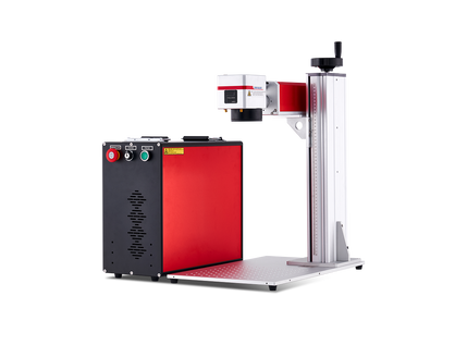
The Three Core Laser Types for Electronics
1. UV Laser (355 nm) — Best for Heat-Sensitive Materials
UV lasers use a photochemical process rather than heat, making them ideal for:
- PCB substrates (FR4, polyimide)
- Plastic IC packages
- Ceramic components
- Silicon wafers
Key advantage: Minimal heat-affected zone (HAZ), preventing damage to delicate materials.

2. Fiber Laser (1064 nm) — Best for Metals
Fiber lasers are widely used for:
- Aluminum enclosures
- Stainless steel housings
- Copper connectors
- Heat sinks
They deliver high-speed, high-contrast marks suitable for production environments.

3. MOPA Fiber Laser — Best for Plated Components
MOPA systems allow precise control over pulse duration, making them essential for:
- Gold-plated connectors
- Nickel-coated semiconductor parts
- Precision electronic contacts
Why it matters: Prevents damage to plating and preserves electrical performance.
Key Applications in Electronics Manufacturing
Printed Circuit Boards (PCBs)
- Materials: FR4, polyimide
- Laser: UV
- Marking: Serial numbers, date codes, 2D codes
PCB marks must survive:
- Reflow soldering (up to 260 °C)
- Cleaning processes
- Conformal coating
Laser marking ensures long-term readability throughout the product lifecycle.

IC Packages & Semiconductor Chips
- Laser: UV or MOPA
- Challenge: Extremely small marking areas
Modern systems can mark a full 2D code in under 50 milliseconds—fast enough for high-volume production without bottlenecks.
SMD Components
- Laser: UV
- Precision: Spot sizes under 10 µm
This enables marking on components as small as 0.6 mm—something no traditional method can achieve.
Connector Terminals
- Laser: MOPA fiber
- Function: Selective plating removal
This replaces chemical etching and improves soldering performance while reducing process steps.
Silicon Wafers
- Laser: UV or green
- Requirement: Zero contamination
Laser marking allows cleanroom-compatible identification without affecting wafer yield.
The Critical Factor: Thermal Control
In electronics, heat isn’t just a variable—it’s a risk.
A slight increase in laser energy can:
- Crack polymer encapsulation
- Distort circuits
- Damage semiconductor junctions
How Modern Systems Solve This
- UV lasers: Use photochemical reactions → minimal heat
- MOPA lasers: Adjustable pulse duration → precise energy control
- Validated parameters: Tailored settings for each material
This is why manufacturers rely on tested application data rather than generic settings.
Integration in Modern Canadian Manufacturing
In Canada, where industries emphasize quality control, traceability, and compliance, laser marking integrates seamlessly with:
- ERP systems
- MES platforms
- Automated production lines
This enables:
- Real-time serialisation
- Batch tracking
- Regulatory compliance (RoHS, CE equivalents, ISO systems)
Why Laser Marking Matters More Than Ever
As electronics become smaller and more complex, traceability requirements continue to grow—especially in sectors like:
- Aerospace
- Medical devices
- Automotive electronics
- Clean energy systems
Laser marking is no longer optional—it’s infrastructure.
Frequently Asked Questions
What is laser marking in electronics?
A non-contact process that permanently marks components with serial numbers, codes, and identifiers that withstand manufacturing and long-term use.
Which laser is best for PCBs?
UV lasers are preferred due to their low thermal impact and high precision.
Can assembled PCBs be laser marked?
Yes. UV lasers can safely mark fully assembled boards without damaging nearby components.
Does laser marking affect performance?
No—when done correctly. Proper parameter settings ensure no impact on electrical or soldering performance.
What information is typically marked?
- Serial numbers
- Date codes
- Batch numbers
- 2D Data Matrix codes
- Compliance marks
In modern electronics manufacturing, a mark smaller than a grain of rice can carry the entire history of a product—from fabrication to field service. Laser marking makes that possible, reliably and permanently.
For Canadian manufacturers balancing precision, compliance, and efficiency, it’s not just a marking method—it’s a foundation for traceability and quality.