


How to Use a Laser Engraver for PCB and Component Labeling
I run a small electronics design studio — three engineers focused on power electronics and motor control boards. For years, we outsourced PCB labeling. Every revision meant delays, minimum order quantities, and extra logistics.
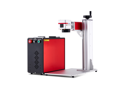
That changed when we installed a fiber laser in-house.

The first job? A batch of 30 development boards — each needing a unique serial number, revision ID, and company logo. Total time: about 40 minutes. No waiting, no back-and-forth. The boards were ready the same day they were assembled.
Looking back, we should have made the switch years earlier.
Across Canada’s growing hardware ecosystem — from Toronto startups to Vancouver prototyping labs — laser engraving has become a practical, scalable solution for PCB identification, prototyping workflows, and small-batch production.

What Is PCB Laser Engraving?
PCB laser engraving (or marking) uses a focused laser beam to create permanent markings on printed circuit boards without physical contact.
These markings can include:
- Serial numbers
- Date codes
- Hardware revisions
- QR / Data Matrix codes
- Logos and branding
- Assembly labels
Unlike ink or labels, laser marks don’t smear, peel, or fade — even after soldering, cleaning, or long-term field use.

Two Use Cases: Fabrication vs. Marking
There are two very different applications:
1. PCB Fabrication (Advanced Use)
Using lasers to remove copper and create circuit traces — typically used in R&D or specialized labs.
2. PCB Marking (Most Common)
Adding permanent identification to finished or semi-finished boards — this is where most Canadian labs, startups, and contract manufacturers benefit.
This guide focuses on marking, which is accessible, cost-effective, and easy to integrate into existing workflows.

Small Canadian Hardware Startup
A six-person IoT company producing 400–600 boards annually used to rely on adhesive labels for traceability.
Problems:
- Labels peeling during assembly
- Misplaced identifiers
- Inconsistent QA tracking
After installing a 30W fiber laser:
- Each board is marked before assembly
- Serial + 2D code added in seconds
- Marks survive soldering and cleaning
Result:
“We haven’t had a traceability issue since. And the boards look far more professional.”
Choosing the Right Laser for PCB Work
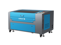
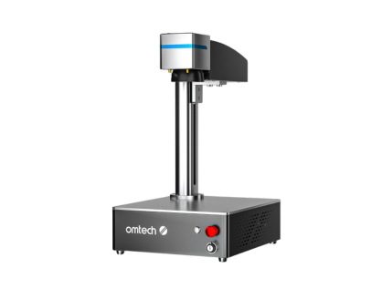
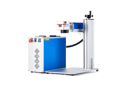
Fiber Laser (Best for Most Canadian Labs)
Wavelength: 1064nm
Best for:
- Dark soldermask PCBs (green, black, blue)
- Metal enclosures
- Batch serial numbering
Why it works:
- High contrast on soldermask
- Fast marking speed
- Works well with LightBurn automation
Ideal for startups, university labs, and small manufacturers.
CO₂ Laser (For Cutting & Light Materials)
Wavelength: 10,600nm
Best for:
- FR4 substrate marking (limited)
- PCB cutting
- Acrylic panels
Important in Canada:
FR4 contains epoxy and brominated compounds. When cut, it releases toxic fumes.
You’ll need:
- Industrial-grade fume extraction
- Proper ventilation (especially in enclosed workshops)
Some Canadian facilities restrict CO₂ PCB cutting entirely due to environmental and safety regulations.
UV Laser (Production-Grade, High Precision)
Wavelength: 355nm
Best for:
- High-end manufacturing
- Assembled PCBs
- Heat-sensitive components
Advantages:
- Minimal heat impact
- Clean, high-precision marks
- Survives reflow soldering (~260°C)
Common in larger EMS providers and regulated industries (medical, aerospace).
Step-by-Step: PCB Labeling Workflow (Fiber Laser + LightBurn)
1. Export Board Design
From tools like KiCad or Eagle:
- Export outline (SVG/DXF)
- Define marking area
2. Set Up Variable Data
In LightBurn:
- Use Variable Text → Serial Number
- Add prefixes (e.g., CA-2026-001)
- Automate batch increments
3. Calibrate Settings
Typical starting points (30W fiber laser):
- Black soldermask: 15–25% power
- Speed: 300–500 mm/s
Always test on scrap boards first.
4. Build a Fixture
- Acrylic jig for alignment
- Multi-board trays for batch runs
Consistency here = speed + accuracy
5. Test First Board
Check:
- Position
- Contrast
- Readability (QR scan test)
6. Run Batch
- Auto-increment serials
- 15–45 seconds per board
- No manual data entry
Common PCB Laser Marking Applications
Date Codes & Revision Tracking
Essential for:
- QA
- Field service
- Warranty tracking
Typical format:
2026-W18 Rev 2.3
2D Codes for Traceability
Widely used in Canadian manufacturing:
- Links to ERP/MES systems
- Tracks production history
Branding & Logos
Important for:
- Investor demos
- Customer-facing hardware
- Product credibility
Assembly Labels
Laser-marked reference designators:
- Reduce assembly errors
- Improve efficiency in small teams
Why Canadian Labs Are Moving In-House
1. Faster Iteration Cycles
No waiting for outsourced labeling.
2. Lower Costs Over Time
No minimum orders or external fees.
3. Better Compliance & Traceability
Supports:
- ISO workflows
- QA documentation
- Product certification processes
4. Professional Appearance
Clean, permanent markings improve perceived product quality.
Systems for PCB Labeling
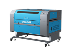
Fiber Laser Systems (Core Choice)
Best for:
- Serial numbers
- Logos
- QR codes
- Batch production
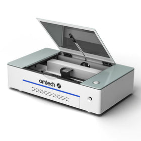
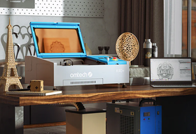
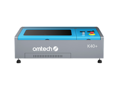
Compact Integrated Systems
Best for:
- Small labs
- Universities
- R&D environments
Canadian-Specific Considerations
🇨🇦 Compliance & Standards
Markings often include:
- CSA (Canadian Standards Association) references
- RoHS / CE / FCC for export products
- Bilingual labeling (English/French) in some markets
Environmental Conditions
Electronics in Canada may face:
- Temperature extremes
- Humidity changes
Laser marks remain stable across these conditions — unlike labels or ink.
Strong Academic & Startup Ecosystem
Laser PCB marking is widely used in:
- University labs
- Hardware accelerators
- Clean tech and robotics startups
Common Mistakes to Avoid
- Using too much power → burns soldermask
- Marking over copper pads → damages functionality
- Skipping test runs
- Using raster images instead of vectors
- Poor ventilation (especially with CO₂ lasers)
For Canadian electronics teams — whether you’re a startup in Toronto, a lab in Montréal, or a contract manufacturer in Ontario — PCB laser engraving is one of the highest ROI upgrades you can make.
It turns labeling from a bottleneck into a fast, in-house, scalable process.